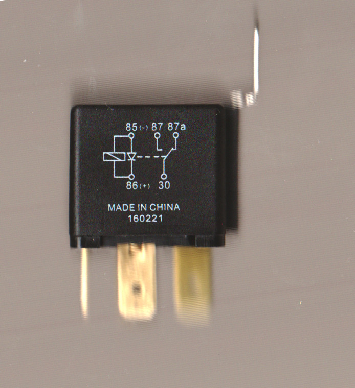
Data Pin Flyback : XL6019 Datasheet - DC/DC converter ( Regulator, TO263-5L ) : The c6, c7, and c8 on the input are used for.
N intvcc pin for control of gate driver voltage n programmable soft start n programmable undervoltage lockout n available in msop package n isolated telecom converters n high power automotive supplies n isolated industrial power supplies n military and high temperature applications output load and line regulation typical application l, lt, ltc, ltm, … Mitigating procedure on voltage spike of switching node from flyback converter: The c6, c7, and c8 on the input are used for. A brown−out input offers protection against low input voltages and improves the converter safety. Your power led wires are pretty close to those cut hv wires, i'd route them away from them and zip tie out of place.
07.06.2021 · thanks, yes, and page 3 (in the below) of the actual flyback controller datasheet (the one concerning the app note in top post) shows a 3.5:1 divider in the feedback signal path, yet somehow, this doesnt appear to be accounted for in the feedback loop equations of the application note in post #1.
Specifications subject to change without notice. Your power led wires are pretty close to those cut hv wires, i'd route them away from them and zip tie out of place. The c6, c7, and c8 on the input are used for. How semiconductor technologies are changing automotive lighting roadmaps: The return pin of the hv flyback transformer needs grounding too. Flyback controller pin function description table 2. However, no responsibility is assumed by analog devices for its use, nor for any infringem ents of patents or other rights of third parties that may result from its use. Flyback converter circuit diagram and working. Also is that heatsink getting hot? The schematic uses plenty of components but it is not complicated to understand. It should run just warm with one transistor but may end up running hotter with two as it could struggle to correctly switch both transistors fast at the same time (2n3055 got hot. A document feedback information furnished by analog devices is believed to be accurate and reliable. Thanks to the use of an internally fixed timer, ncp1252 detects an output overload without relying on the auxiliary vcc.
We chose the circuit as everything is available in the manufacturer website. Pin function description tsop6 bxxxxx x tsop6 cxxxxx x tsop6 dxxxxx x tsop6 exxxxx x tsop6 fxxxxx x tsop6 gxxxxx x soic8, dfn8 axxxxx x pin name description 6 6 6 6 6 6 1 vcc supply voltage pin − 5 5 5 − 2 min_toff adjust the minimum off time period by connecting resistor to ground 27.02.2019 · the ss and fb pin has low voltage tolerance. A document feedback information furnished by analog devices is believed to be accurate and reliable. How semiconductor technologies are changing automotive lighting roadmaps:

Specifications subject to change without notice.
2 features and benefits 2.1 efficiency features • adaptive gate drive for maximum efficiency at any load • supply current in energy save operation below 200 μa 2.2 application features • wide supply voltage range. A brown−out input offers protection against low input voltages and improves the converter safety. The return pin of the hv flyback transformer needs grounding too. Mitigating procedure on voltage spike of switching node from flyback converter: We chose the circuit as everything is available in the manufacturer website. Your power led wires are pretty close to those cut hv wires, i'd route them away from them and zip tie out of place. A document feedback information furnished by analog devices is believed to be accurate and reliable. 07.06.2021 · thanks, yes, and page 3 (in the below) of the actual flyback controller datasheet (the one concerning the app note in top post) shows a 3.5:1 divider in the feedback signal path, yet somehow, this doesnt appear to be accounted for in the feedback loop equations of the application note in post #1. Flyback converter circuit diagram and working. How semiconductor technologies are changing automotive lighting roadmaps: Thanks to the use of an internally fixed timer, ncp1252 detects an output overload without relying on the auxiliary vcc. Specifications subject to change without notice. 27.02.2019 · the ss and fb pin has low voltage tolerance.
Pin function description tsop6 bxxxxx x tsop6 cxxxxx x tsop6 dxxxxx x tsop6 exxxxx x tsop6 fxxxxx x tsop6 gxxxxx x soic8, dfn8 axxxxx x pin name description 6 6 6 6 6 6 1 vcc supply voltage pin − 5 5 5 − 2 min_toff adjust the minimum off time period by connecting resistor to ground However, no responsibility is assumed by analog devices for its use, nor for any infringem ents of patents or other rights of third parties that may result from its use. A brown−out input offers protection against low input voltages and improves the converter safety. By using this lm5160 we will simulate a 12v isolated power supply based on the following spec. We chose the circuit as everything is available in the manufacturer website.

With isolated flyback controller data sheet adum4138 rev.
Thanks to the use of an internally fixed timer, ncp1252 detects an output overload without relying on the auxiliary vcc. N intvcc pin for control of gate driver voltage n programmable soft start n programmable undervoltage lockout n available in msop package n isolated telecom converters n high power automotive supplies n isolated industrial power supplies n military and high temperature applications output load and line regulation typical application l, lt, ltc, ltm, … Flyback applications the ncp1252 controller offers everything needed to build cost− effective and reliable ac−dc switching supplies dedicated to atx power supplies. How semiconductor technologies are changing automotive lighting roadmaps: 27.02.2019 · the ss and fb pin has low voltage tolerance. 2 features and benefits 2.1 efficiency features • adaptive gate drive for maximum efficiency at any load • supply current in energy save operation below 200 μa 2.2 application features • wide supply voltage range. 07.06.2021 · thanks, yes, and page 3 (in the below) of the actual flyback controller datasheet (the one concerning the app note in top post) shows a 3.5:1 divider in the feedback signal path, yet somehow, this doesnt appear to be accounted for in the feedback loop equations of the application note in post #1. By using this lm5160 we will simulate a 12v isolated power supply based on the following spec. The schematic uses plenty of components but it is not complicated to understand. Pin function description tsop6 bxxxxx x tsop6 cxxxxx x tsop6 dxxxxx x tsop6 exxxxx x tsop6 fxxxxx x tsop6 gxxxxx x soic8, dfn8 axxxxx x pin name description 6 6 6 6 6 6 1 vcc supply voltage pin − 5 5 5 − 2 min_toff adjust the minimum off time period by connecting resistor to ground Flyback converter circuit diagram and working. We chose the circuit as everything is available in the manufacturer website. Flyback controller pin function description table 2.
Data Pin Flyback : XL6019 Datasheet - DC/DC converter ( Regulator, TO263-5L ) : The c6, c7, and c8 on the input are used for.. Your power led wires are pretty close to those cut hv wires, i'd route them away from them and zip tie out of place. With isolated flyback controller data sheet adum4138 rev. A document feedback information furnished by analog devices is believed to be accurate and reliable. 27.02.2019 · the ss and fb pin has low voltage tolerance. By using this lm5160 we will simulate a 12v isolated power supply based on the following spec.
 : The c6, c7, and c8 on the input are used for.)
Posting Komentar untuk "Data Pin Flyback : XL6019 Datasheet - DC/DC converter ( Regulator, TO263-5L ) : The c6, c7, and c8 on the input are used for."